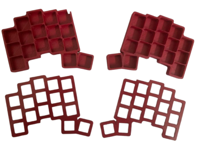
Hi, I have finally started working on my own handwired keyboard. I have been wanting to build a split keyboard for a while, inspired by r/MechanicalKeyboards, and I finally decided to take the leap. I don't know how to touch type, so that will be a challenge for me, but I am excited to learn. Starting off, the main choices are the number of keys, the layout, PCB design, the case, the switches, the keycaps, the wires, and the microcontroller. Since it is my first time building a keyboard, I decided to go with the simplest options for connection and assembly: a wired connection and a 34-key split ortholinear layout like the Sweep (17 keys per half).
I did not want to spend time and money on designing a PCB, especially since the minimum order quantity (MOQ) for them is usually 5 in Indian fabrication stores, so I chose a handwired design instead. In traditional handwired keyboards, switches are usually arranged in a row-and-column matrix to use significantly fewer pins. However, a matrix design can cause ghosting and key rollover issues, which is why people have to add diodes to every single switch to prevent that. I wanted to keep things minimal and avoid the hassle of soldering 34 individual diodes, so I decided to bypass the matrix entirely and go with a direct connection design, where each switch connects straight to its own dedicated GPIO pin on the microcontroller.
Finding documentation for a purely handwired Ferris Sweep build was difficult, so I decided to design the case myself. My experience with 3D modeling was limited to a few basic prints, so I was not entirely sure how to go about designing a case from scratch. Since my goal is to keep things simple so I can debug issues easily, I try to find open-source tools and resources wherever possible to see exactly how things are done instead of just copying them blindly. That is when I found ergogen.xyz, an open-source website that converts YAML configuration code to geometry.
They have templates for split keyboards, so I modified a Sweep-like YAML template to output just the case and switch plate files. Since I am handwiring, I didn't need to worry about the PCB design. I settled on a two-piece housing consisting of a 1mm top mounting plate and a bottom case with an 8mm depth to clear the wiring. The switch plate STL, bottom case STL, and ergogen YAML files are linked inline.
After discussing with a few vendors to keep the budget low, I went with a local vendor who charged me about 500 INR for printing the case and plate in PLA with 10% infill. The print took about 7 hours, and I got the parts back in a single day with decent quality.
Now it is time to order the rest of the parts. Because I am going with a diodeless, direct-pin design, I have to be careful with my component selection—especially when it comes to finding microcontrollers that have enough available pins for each half while still fitting inside the case. I will map out my complete component list, specific part choices, and the final budget breakdown in a separate bill of materials update next.